 New 3D-stacked memory cells can revolutionize the concept of memory chips
By Kiran N. Kumar
From huge memory floppy disks to compact discs to flash drives, the size of computer media formats and memory devices have constantly been shrinking.
Japanese scientists, who had pioneered the miniaturization of floppy disks to CDs, have once again scored a milestone developing a new 3D-stacked memory cell that can revolutionize the concept of memory chips.
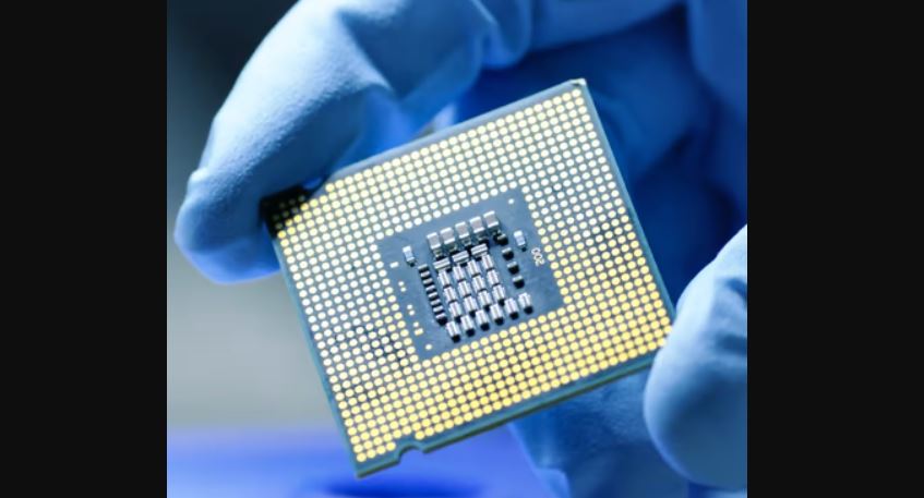
As the new machine learning, artificial intelligence (AI) and Big Data are the new buzz words in the tech world, mobile cloud-enabled devices require greater memory that is energy-efficient and smaller in size.
Read: Rechargeable batteries: Search on for safer, faster, high energy storage devices (June 7, 2022)
Currently, flash memory devices require relatively large currents to read or write data that will change with the new 3D memory devices.
Making a headway in the direction, a team of researchers of the Institute of Industrial Science at the University of Tokyo have fabricated three-dimensional vertically formed field-effect transistors to produce high-density data storage devices.
This proof-of-concept 3D stacked memory cell is based on ferroelectric and antiferroelectric field-effect transistors (FETs) with atomic-layer-deposited oxide semiconductor channels.
These FETs can store ones and zeros in a non-volatile manner, without the requirement for power all the time. It means the vertical device structure increases information density and reduces operation energy needs.
By depositing hafnium oxide and indium oxide layers in a vertical trench structure, they made ferroelectric materials with electric dipoles that are most stable when aligned in the same direction.
In addition, ferroelectric Hafnium Oxide spontaneously enables the vertical alignment of the dipoles. Information is stored by the degree of polarization in the ferroelectric layer, which can be read by the system owing to changes in electrical resistance.
On the other hand, antiferroelectrics like to alternate the dipoles up and down in the erased state, enabling efficient erasure operations within the oxide semiconductor channel, said the scientists.
To be precise, by using antiferroelectric instead of ferroelectric, they found that only a tiny net charge was required to erase data, which leads to more efficient write operations. Hence, the road ahead allows for new even smaller and more eco-friendly data-storage devices.
“We showed that our device was stable for at least 1,000 cycles,” said lead author Zhuo Li. The team experimented with various thicknesses for the indium oxide layer and found that optimizing this parameter can lead to significant increases in performance.
Read: Building Up New Data-Storage Memory (June 13, 2022)
The researchers also used first-principles of computer simulations to plot the most stable surface states.
“Our approach has the potential to greatly improve the field of non-volatile memory,” senior author Masaharu Kobayashi says. This kind of research using both experimental prototypes coupled with computer simulations may help enable future consumer electronics.
The work has been published in 2022 IEEE Silicon Nanoelectronics Workshop on High-Density Memory.